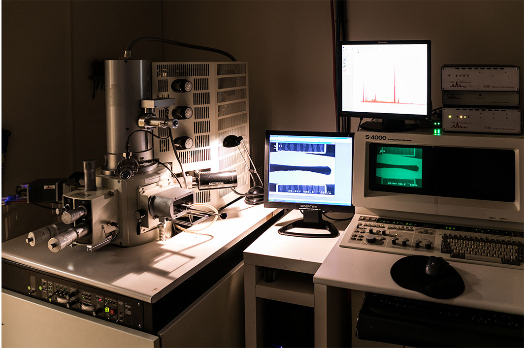
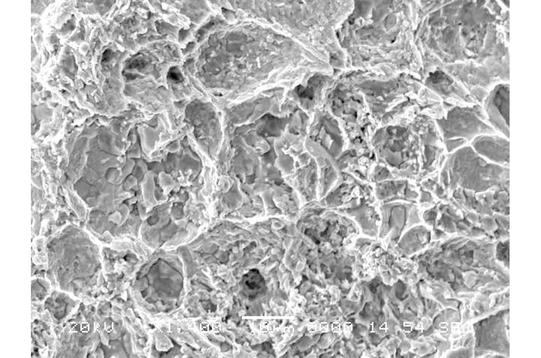
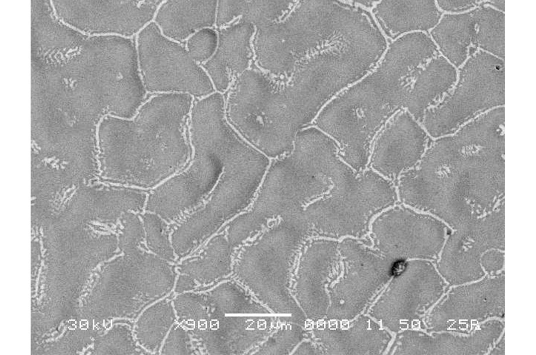
Our Hitachi S4000 Field Emission and Jeol JSM-5800 LV Scanning Electron Microscopes (SEM), each equipped with an Energy Dispersive X-ray Microanalysis system (EDS) allow for capturing of high-resolution images up to x200000 in accordance with customer requirements. An extra-large chamber of our Jeol SEM, allows for large objects to be investigated, while its low vacuum (LV) feature allows for observation of very fragile (for instance biological) objects.
A wide range of applications utilizes SEM, partly because of the ease and less destructive nature of sample preparation and unprecedented depth of field, compared to light microscopy. Depending on the task, as-received or specially prepared cross-sectioned samples can be inspected.


